

JTAG 2 - How JTAG works
Now that we know how to connect JTAG to different ICs, let's see in detail how JTAG works and how to control it from a PC.
Control JTAG from your PC
You use a "JTAG cable" to control a JTAG bus from a PC. The JTAG cable is just a way to control the four JTAG signals from the PC. The JTAG cable might connect to a PC's parallel (printer) port, USB port or Ethernet port... The simplest is a parallel port (available only on older PCs unfortunately). USB and Ethernet JTAG cables are good too. They are faster at streaming large amount of data, but more complex to control and with more overhead (=slower) for small amount of data.
The parallel port
A parallel port can be regarded as a twelve-bit output from the PC, and a five-bit input to the PC. JTAG just requires a three-bit output and a one bit input. For example, take a look at the schematic of Xilinx's parallel-III cable. You can see on the left the PC's parallel signals, one the right the JTAG connector, and in the middle a few 74HC125 buffers.
From the software point of view, a parallel port is ideal since it is very easy to control.
For example, here's C code that shows how to toggle the TCK signal for an Altera ByteBlaster JTAG cable.
#define lpt_addr 0x378
#define TCK 0x01

void toggle_TCK()
{
	outport(lpt_addr, 0);
	outport(lpt_addr, TCK);
	outport(lpt_addr, 0);
}
One minor problem with Windows 2000/XP/Vista is that the "outport" IO instruction is restricted, but GiveIO and UserPort are free generic drivers that open up the IO space.
The JTAG TAP controller
We know that a PC is connected to the JTAG bus as illustrated here:
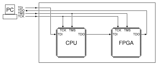
So we have 4 signals (TDI, TDO, TMS, TCK) to take care of.
TCK
That's the JTAG clock signal. The other JTAG signals (TDI, TDO, TMS) are synchronous to TCK. So TCK has to toggle for anything to happen (usually things happen on TCK's rising edge).
TMS
Inside each JTAG IC, there is a JTAG TAP controller. On the figure above, that means that there is a TAP controller in the CPU and another in the FPGA.
The TAP controller is mainly a state machine with 16 states. TMS is the signal that controls the TAP controller. Since TMS is connected to all the JTAG ICs in parallel, all the TAP controllers move together (to the same state).
Here's the TAP controller state machine:
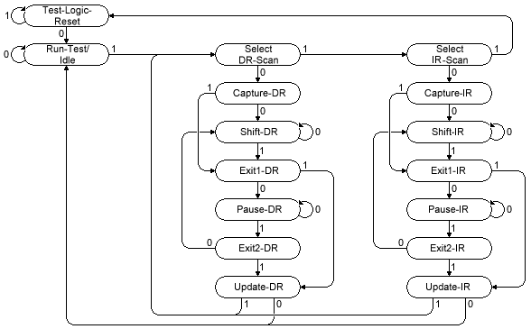
The little numbers ("0" or "1") close to each arrow are the value of TMS to change state. So for example, if a TAP controller is at state "Select DR-Scan" and TMS is "0" and TCK toggles, the state changes to "Capture-DR".
The tap controllers must always be in the same state, although after power-up they may be in a random state... but there is a trick. Look at the state machine and notice that no matter what state you are, if TMS stays at "1" for five clocks, a TAP controller goes back to the state "Test-Logic-Reset". That's used to synchronize the TAP controllers.
So let's say we want to go to "Shift-IR" after power-up:
	// first sync everybody to the test-logic-reset state
	for(i=0; i<5; i++) JTAG_clock(TMS);

	// now that everybody is in a known and identical state, we can move together to another state
	// let's go to Shift-IR
	JTAG_clock(0);
	JTAG_clock(TMS);
	JTAG_clock(TMS);
	JTAG_clock(0);
	JTAG_clock(0);
TDI and TDO
Now that we know how to change state, we can use the two most important JTAG states, namely "Shift-DR" and "Shift-IR".
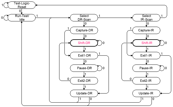
Shift-DR and Shift-IR are used in combination with the TDI and TDO lines.
Let's start with Shift-IR.
There is one register into each IC TAP controller called IR, the "instruction register". You write a value into this register that corresponds to what you want to do with JTAG (each IC has a list of possible instructions).
Also each IC IR register has a specific length. For example, let's say that the CPU's IR is 5 bits long, and the FPGA's IR is 10 bits long. The IR registers form a chain that is loaded through the TDI and TDO pins.
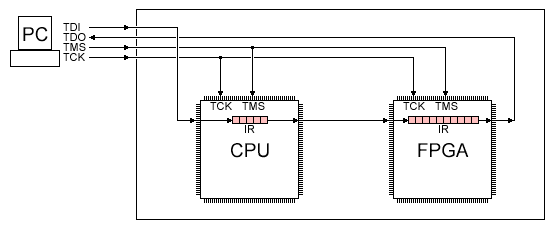
From the PC point of view, the above IR chain is 15 bits long.
To load IR values, the PC has to make sure the TAP controllers are in the Shift-IR state, and send 15 bits through TDI.
Once shifted, the first 10 bits actually end up into the FPGA IR, and the last 5 bits into the CPU IR.
If the PC was sending more than 15 bits, it would start receiving what it sent earlier on TDO.
For example, let's send 00100 into the CPU's IR, and 0000000010 into the FPGA's IR.
	// Because the bits are shifted through in a chain, we must start sending the data for the device that is at the end of the chain
	// so we send the 10 FPGA IR bits first
	JTAG_clock(0);
	JTAG_clock(1);
	JTAG_clock(0);
	JTAG_clock(0);
	JTAG_clock(0);
	JTAG_clock(0);
	JTAG_clock(0);
	JTAG_clock(0);
	JTAG_clock(0);
	JTAG_clock(0);

	// then send the 5 CPU IR bits
	JTAG_clock(0);
	JTAG_clock(0);
	JTAG_clock(1);
	JTAG_clock(0);
	JTAG_clock(0 | TMS);	// last bit needs to have TMS active (to exit shift-IR)
In our example, the CPU's IR is 5 bits long (i.e. can hold values from 0 to 31). That means it can support up to 32 JTAG instructions. In practice, a CPU probably uses 5 to 10 instructions, and the remaining IR values are unused.
Same thing for the FPGA, with a 10-bit long IR, it can hold 1024 instructions, with most of them unused.
JTAG has a few mandatory instructions (what these instructions do will be illustrated later):
- BYPASS
- EXTEST
- SAMPLE/PRELOAD
- IDCODE (not mandatory but very often implemented)
To get the list of possible IR values supported by a specific IC, check the IC's datasheet (or BSDL file - more on that later).
DR registers
Each TAP controller has only one IR register, but has multiple DR registers. The DR registers are similar to the IR registers (they are shifted the same way the IR registers are but using the Shift-DR state instead of the Shift-IR).
Each IR value selects a different DR register. So in our example, the CPU could have up to 32 DR registers (if all IR instructions were implemented).