

PCI 1 - How PCI works
We concentrate on PCI 2.2 32-bit here, which is what is used in today's PCs.
Newer PCI versions include PCI 2.3 and PCI 3.0.
Unlike the Ethernet specification, the PCI specification cannot be downloaded for free. You need to be a member of the PCI-SIG to access the specification. As becoming a member is expensive, you might want to check your company's hardware group (assuming you work in the semiconductor industry) to see if you can get access to the specification.
Otherwise here's a short introduction, followed by some links for more info.
While the host CPU is often the bus master, all PCI boards can potentially claim the bus and become a bus master.
When a transaction starts, the master specifies the starting address of the transaction, if it's a read or a write, AND which space he wants to speak to.
That's because CPUs typically don't "speak" PCI natively, so a bridge has to translate the transactions from the CPU's bus to the PCI's bus. Also CPUs never have 3 memory spaces like PCI devices. Most CPUs have 1 space (memory space), while other CPUs have 2 (memory & IO). The bridge has to play some tricks so that the CPU can still access all 3 PCI spaces.
PCI board connectors have one or two slots that identify if the board is 3.3V or 5V compliant. This is to ensure that, for example, a 3.3V only board cannot be plugged into a PC's 5V-only PCI bus.
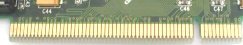
Here an example of 5V-only board:
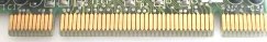
while this board is both 5V and 3.3V compliant:
With a 33MHz clock, we have:
Newer PCI versions include PCI 2.3 and PCI 3.0.
The PCI specification
The PCI is developed and maintained by a group called the PCI Special Interest Group (PCI-SIG in short).Unlike the Ethernet specification, the PCI specification cannot be downloaded for free. You need to be a member of the PCI-SIG to access the specification. As becoming a member is expensive, you might want to check your company's hardware group (assuming you work in the semiconductor industry) to see if you can get access to the specification.
Otherwise here's a short introduction, followed by some links for more info.
PCI characteristics
The PCI bus has 4 main characteristics:- Synchronous
- Transaction/Burst oriented
- Bus mastering
- Plug-and-play
PCI is synchronous
The PCI bus uses one clock. The clock runs at 33MHz by default but can run lower (all the way down to idle = 0MHz) to save power, or higher (66MHz) if your hardware supports it.PCI is Transaction/Burst oriented
PCI is transaction oriented.- You start a transaction
- You specify the starting address (one clock cycle)
- You send as many data as you want (many following clock cycles)
- You end the transaction
PCI allows bus mastering
PCI transactions work in a master-slave relationship. A master is an agent that initiates a transaction (can be a read or a write).While the host CPU is often the bus master, all PCI boards can potentially claim the bus and become a bus master.
PCI is plug-and-play
PCI boards are plug-and-play. That means that the host-CPU/host-OS can:- Determine the identity of each PCI board in a PCI bus (manufacturer & function (video, network...))
- Determine the abilities/requirements of each board (how much memory space it requires, how many interrupts...)
- Relocate each board memory space
PCI "spaces"
PCI defines 3 "spaces" where you can read and write.When a transaction starts, the master specifies the starting address of the transaction, if it's a read or a write, AND which space he wants to speak to.
- Memory space
- IO space
- Configuration space
- The memory and IO spaces are the workhorse spaces. They are "relocatable" (i.e. the addresses at which each board responds can be moved).
- The configuration space is used for plug-and-play.
It's a space where each board has to implement very specific registers at very specific addresses, so that the host-CPU/OS can figure out what is each board's identity/abilities/requirements.
From there, the host CPU/OS enables and configures the other two spaces.
This space is fixed and always starts at address 0 for all PCI boards; so one line of the PCI connector is used as board-select (for this space only).
PCI bridge
PCI devices don't connect directly to a host CPU, but go through a "bridge" chip.That's because CPUs typically don't "speak" PCI natively, so a bridge has to translate the transactions from the CPU's bus to the PCI's bus. Also CPUs never have 3 memory spaces like PCI devices. Most CPUs have 1 space (memory space), while other CPUs have 2 (memory & IO). The bridge has to play some tricks so that the CPU can still access all 3 PCI spaces.
PCI voltage
PCI boards can use 3.3V or 5V signaling. Interestingly, current PCs all use 5V signaling.PCI board connectors have one or two slots that identify if the board is 3.3V or 5V compliant. This is to ensure that, for example, a 3.3V only board cannot be plugged into a PC's 5V-only PCI bus.
Here an example of 5V-only board:
while this board is both 5V and 3.3V compliant:
PCI timing
PCI specifies timing related to its clock.With a 33MHz clock, we have:
- 7ns/0ns Tsu/Th (setup/hold) constraint on inputs
- 11ns Tco (clock-to-output) on outputs
Links
- A short PCI Bus Operation page.
- Also An Experiment to Build a PCI Board